Conduction Loss
In the conduction state, the switch does have a small resistance and voltage drop across it, and the switch dissipates power as a function of the current flowing through it.
For a MOSFET, this power is typically modeled as:
P = ID2 * RDSon = ID * VDS
- where ID is the Drain current,
- RDSon is the dynamic on-resistance between the Drain and the Source, often < 1 W, and
- VDS is the saturation voltage between the Drain and the Source, often < 1 V
For an IGBT or BJT, this power is typically modeled as:
P = IC * VCEsat
- where IC is the Collector current and
- VCEsat is the saturation voltage between the Collector and the Emitter, often < 1 V
Turn-on Loss
During turn-on, the current through the switch rapidly increases and the voltage drop across the device quickly decreases. However, parasitic elements, such as the Gate-to-Drain capacitance in a MOSFET, prevent the switch from turning on instantaneously. While the device is turning on, there is significant current flowing through the device and significant voltage across the device, and significant power loss occurs.
For a MOSFET, during turn-on, this power is typically modeled as:
P = ID * VDS
- where ID is the Drain current and
- VDS is the voltage between the Drain and the Source
For an IGBT or BJT, during turn-on, this power is typically modeled as:
P = IC * VCE
- where IC is the Collector current and
- VCE is the Collector to Emitter voltage
Turn-off Loss
In a similar manner, during turn-off, the current through the switch rapidly decreases and the voltage drop across the device quickly increases, but circuit parasitics prevent the switch from turning off instantaneously. While the device is turning off, there is significant current flowing through the device and significant voltage across the device, and significant power loss occurs. The equations above also apply.
Measuring Switching Loss
There are two approaches to measuring switching loss: it can be measured using manual setups and built-in oscilloscope measurements, but there are also automated measurement systems available on some oscilloscopes. The automated measurements have the advantages of being easy to set up and delivering easily repeatable results. With either technique, careful probing and optimization will help you get good results.
Probing and Measurement Setup
Before discussing the specific power measurements, there are six key steps to making accurate and repeatable measurements:
1. Remove voltage offset errors: The amplifiers in differential probes may have a slight DC voltage offset which will affect measurement accuracy. With the inputs shorted and no signals applied, automatically or manually adjust the DC offsets in the probe to zero.
2. Remove current offset errors: Current probes may also exhibit DC offset errors due to residual magnetism in probe, as well as amplifier offsets. With the jaws closed and no signals applied, automatically or manually null out the DC offsets in the probe.
3. Remove timing errors: Because instantaneous power measurements are calculated based on multiple signals, it is important that the signals be properly time-aligned. Different technologies are used to measure voltages and currents, and the propagation delays through these devices may be significantly different, leading to measurement errors. Good results are generally possible by adjusting the inter-channel timing to account for the difference in nominal propagation delays in the deskew menu. For the most accurate results, apply a high-slew-rate signal to all inputs and carefully remove any relative timing offset (skew) between all channels.
4. Optimizing Signal-to-Noise Ratio: In all measurement systems, but especially in digital devices such as modern oscilloscopes, good measurement technique requires keeping signals as large as possible (without clipping) to minimize the effects of noise and to maximize vertical resolution. This includes using the lowest necessary attenuation when probing the signals and using the full dynamic range of the oscilloscope.
5. Signal conditioning: Measurement quality can also be improved by conditioning the input signals. Bandwidth limiting can be used to selectively reduce noise above the frequencies of interest, and averaging can be used to reduce uncorrelated or random noise on the signal. High Res acquisition mode provides bandwidth limiting and noise reduction, increased vertical resolution, and it even works on signals acquired in single shot mode.
6. Accuracy and safety: For best accuracy, be sure to use the equipment within the normal operating range and below the peak ratings. And, for your safety, always stay well within the equipment’s absolute maximum specifications and follow manufacturer's instructions for use.
Measuring Switch Loss - Manual Setup and Built-in Measurements
One way to measure turn-off loss is with gated measurements. The object is to measure the average power dissipated during the turn-off phase. In this example, the MOSFET's VDS is acquired with a differential voltage probe and is shown in yellow in Figure 4. The Drain current is acquired with an AC/DC current probe and is shown in cyan. The vertical sensitivity and offset of each channel is adjusted so the signals occupy more than half of the vertical range, but without extending beyond the top and bottom of the graticule.



 400-616-5217


 Vị trí hiện tại:
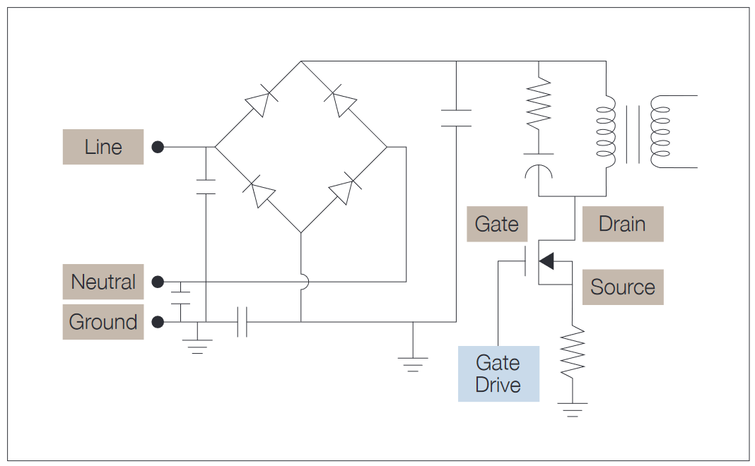 Figure 1. Simplified switch mode power supply switching circuit.
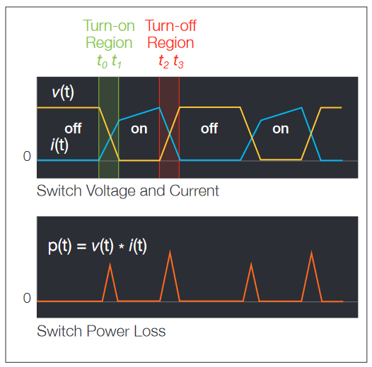 Figure 2. Multiplying instantaneous voltage across and current through a switching device gives instantaneous power throughout the switching cycle.
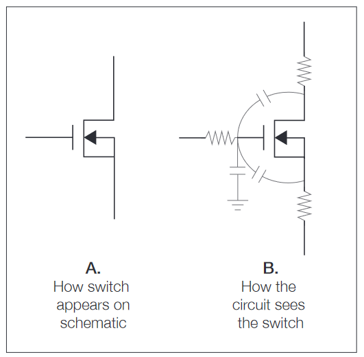 Figure 3. A: How the switch appears on the schematic, and B: How the circuit sees the switch.
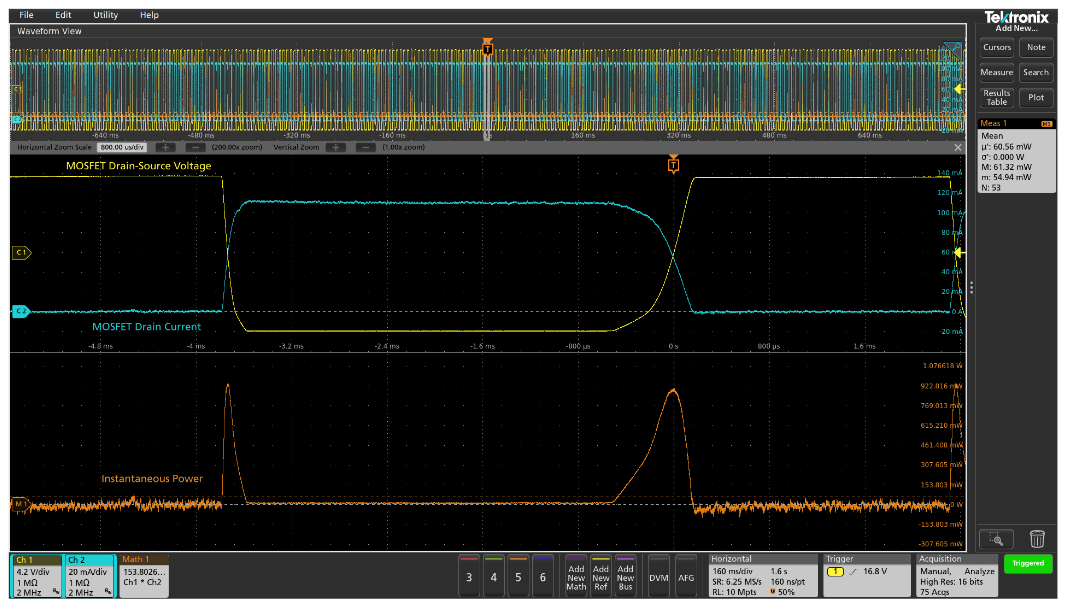 Figure 4. Switching power loss measurement using waveform multiplication and mean measurement on the power data over the whole acquisition. This technique relies on manual setup, using standard capabilities of this oscilloscope.
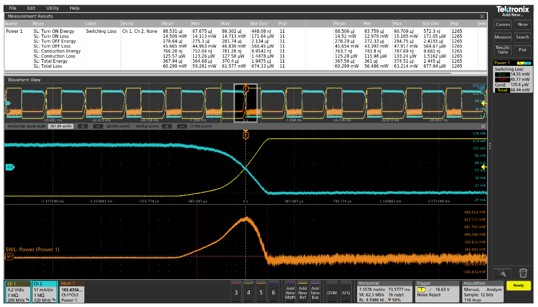 Figure 5. Automated switching loss measurement determines power and energy loss during turn-on, turn-off, and conduction. In this case the power analysis software automatically sets up the measurement when the Switching Loss measurement is turned on.
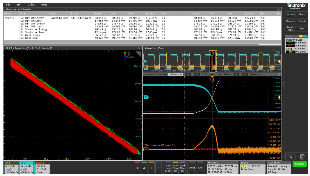 Figure 6. A trajectory plot shows voltage versus current during turn-on (green traces) and turn-off (red traces) over many cycles, showing how switching changes over time. In this test circuit the drain current is limited by resistors, so the plots are linear.
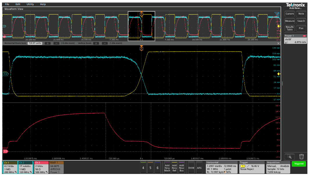 Figure 7. Automated slew rate measurement on a MOSFET gate signal.
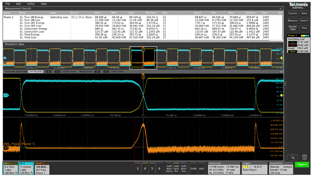 Figure 8. Automated switching loss measurement, showing significant improvement.



 粤公网安备 44030502008393号